File:Generic block diagram of a GPU.svg
Jump to navigation
Jump to search

Size of this PNG preview of this SVG file: 639 × 600 pixels. Other resolutions: 256 × 240 pixels | 512 × 480 pixels | 818 × 768 pixels | 1,091 × 1,024 pixels | 2,182 × 2,048 pixels | 650 × 610 pixels.
Original file (SVG file, nominally 650 × 610 pixels, file size: 36 KB)
Summary
| Description |
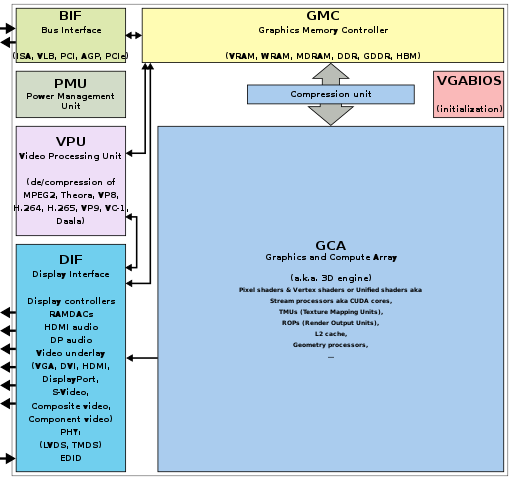
English: Generic block diagram of a GPU as found on modern graphics cards. The Wikipedia contains separate articles to many of the depicted components and used communication protocols. BIF: ISA (Industry Standard Architecture), VLB (VESA Local Bus), PCI (Peripheral Component Interconnec), AGP (Accelerated Graphics Port), PCIe |
| Date | |
| Source | Own work |
| Author | ScotXW |
| Other versions |
for a general idea on the usage of rendering APIs (OpenGL, Direct3D, Vulkan) cf.  |
Licensing
| This file is made available under the Creative Commons CC0 1.0 Universal Public Domain Dedication. | |
| The person who associated a work with this deed has dedicated the work to the public domain by waiving all of their rights to the work worldwide under copyright law, including all related and neighboring rights, to the extent allowed by law. You can copy, modify, distribute and perform the work, even for commercial purposes, all without asking permission.
|
File history
Click on a date/time to view the file as it appeared at that time.
| Date/Time | Thumbnail | Dimensions | User | Comment | |
|---|---|---|---|---|---|
| current | 12:24, 25 November 2019 | | 650 × 610 (36 KB) | commons>Mhare | File uploaded using svgtranslate tool (https://tools.wmflabs.org/svgtranslate/). Added translation for bs. |
File usage
There are no pages that use this file.