File:GaP-wafer.jpg
Jump to navigation
Jump to search

Size of this preview: 800 × 576 pixels. Other resolutions: 320 × 230 pixels | 640 × 461 pixels | 1,024 × 737 pixels | 1,280 × 921 pixels | 1,776 × 1,278 pixels.
Original file (1,776 × 1,278 pixels, file size: 300 KB, MIME type: image/jpeg)
File history
Click on a date/time to view the file as it appeared at that time.
| Date/Time | Thumbnail | Dimensions | User | Comment | |
|---|---|---|---|---|---|
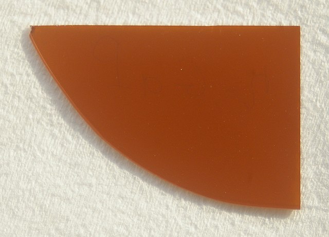
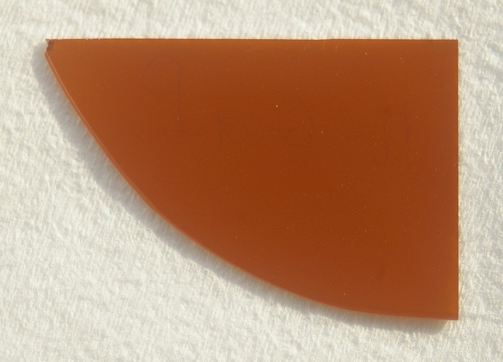
| current | 08:56, 13 October 2019 | | 1,776 × 1,278 (300 KB) | commons>Materialscientist | {{Information |description ={{en|1=GaP wafer, one-side polished, S-doped n-type, sample length ~2 cm, thickness 0.430 mm}} |date =2019-10-13 |source ={{own}} |author =Materialscientist }} == {{int:license-header}} == {{self|cc-by-sa-4.0|GFDL}} Category:Gallium compounds Category:Photographs by User:Materialscientist |
File usage
There are no pages that use this file.